Experience across 3nm to 180nm process nodes with major foundry ecosystems.
Best-in-class Performance, Power, and Area results through advanced techniques.
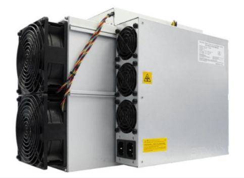
Successful tapeouts for AI accelerator, GPU, DTV SoC, automotive and mining ASICs.
The team has design experience across process nodes from 3nm to 180nm, covering major fabs including:
DVFS, clock gating, power gating, multi-domain power optimization.

Best-in-class Performance, Power, and Area results through advanced techniques.
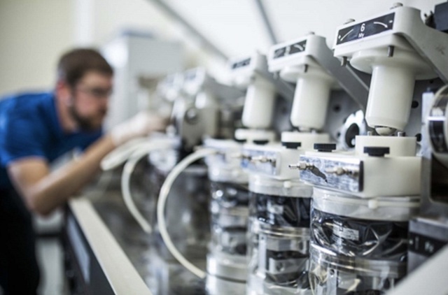
100+ custom automation scripts and comprehensive quality checks.
Complete signoff flow including timing, power, reliability, and DRC.
AI inference chip for cloud and edge computing. FP32 2.2 TFlops, INT8 17.6 TOPS (35.2 TOPS with Winograd), 16W typical power consumption.
Ultra-high-definition digital TV chip with 8K60 output, HDMI 2.1, AVS3 decoding support, quad-core 64-bit processor delivering 36K+ DMIPS.
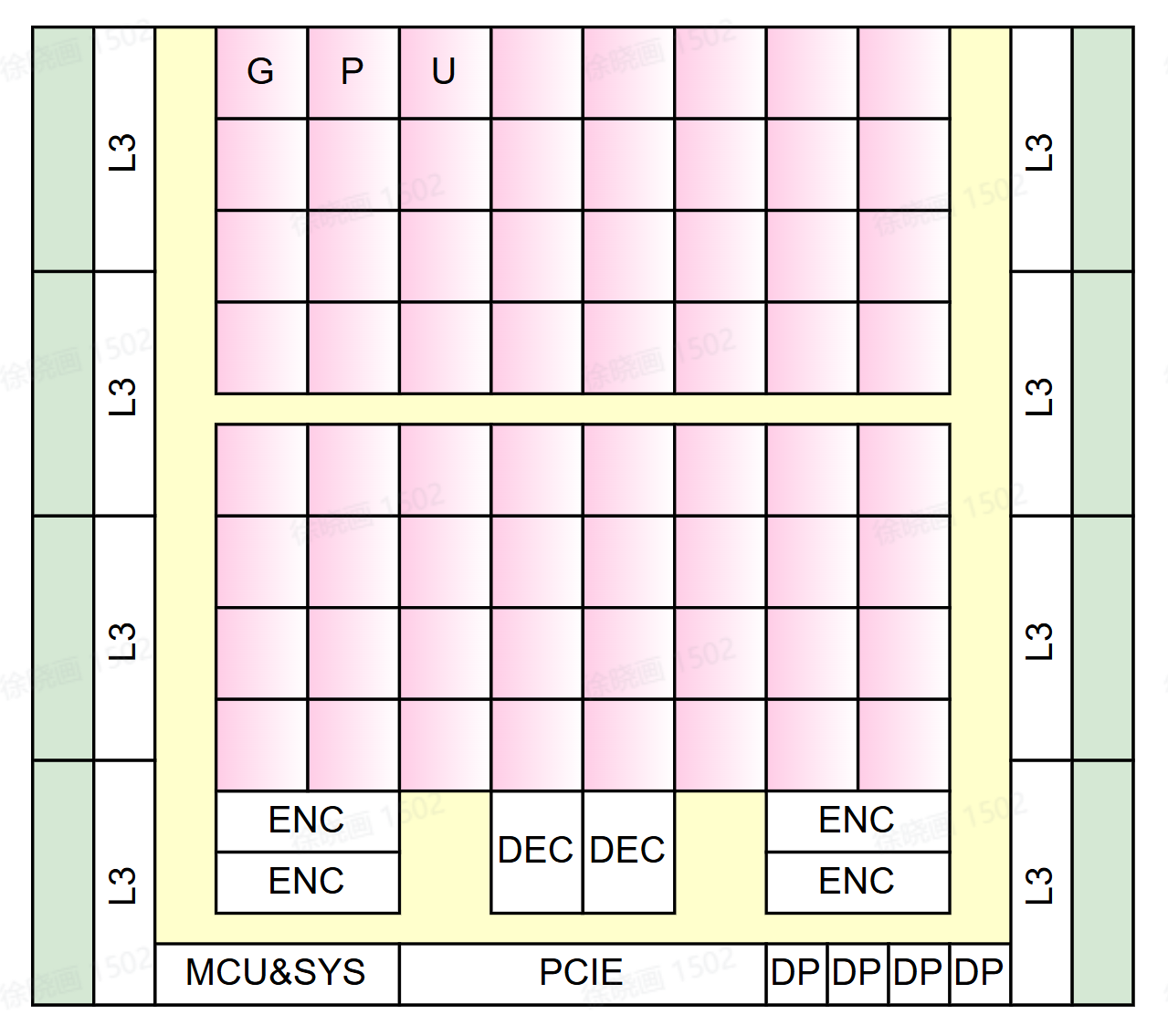
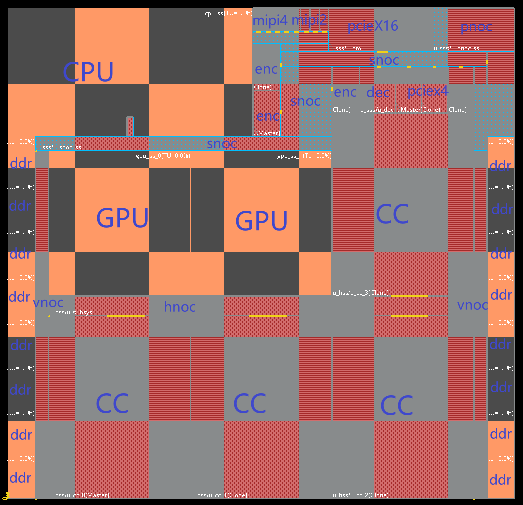
High-performance GPU with 64 cores, GDDR6 x8 @16Gbps, PCIe Gen4x16, 4K encoder + 2 decoder channels, 20x20mm package.
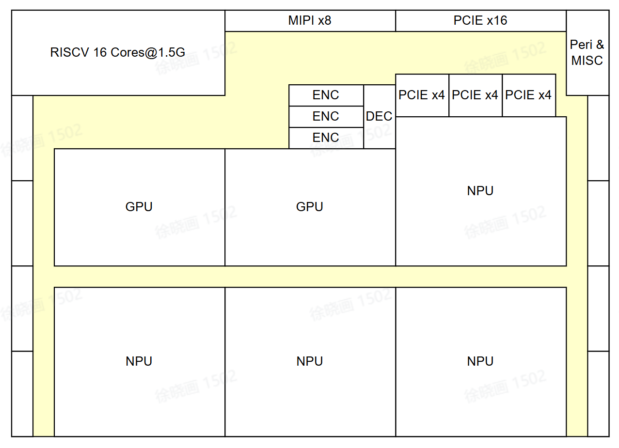
RISC-V 16-core CPU with LPDDR5@6400, NPU x4, GPU x2, MIPI x8, PCIe interfaces, 25x25mm package for autonomous driving.
Production mining machine with 8.2 TH/s hashrate, 3050W power consumption, 372 J/T efficiency, 276 hash chips across 3 boards.
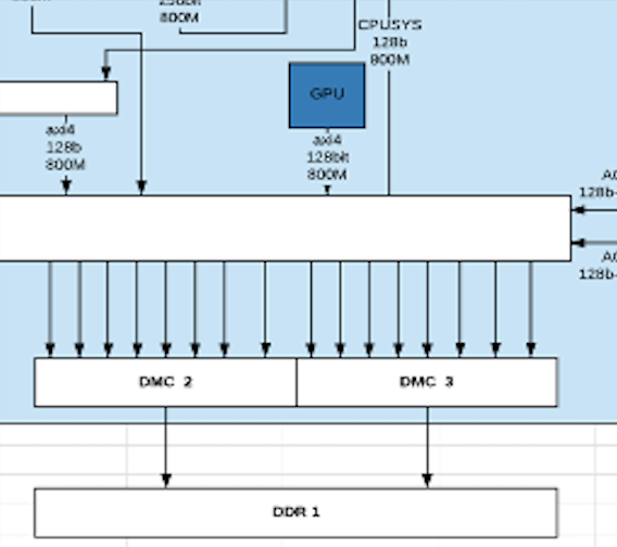
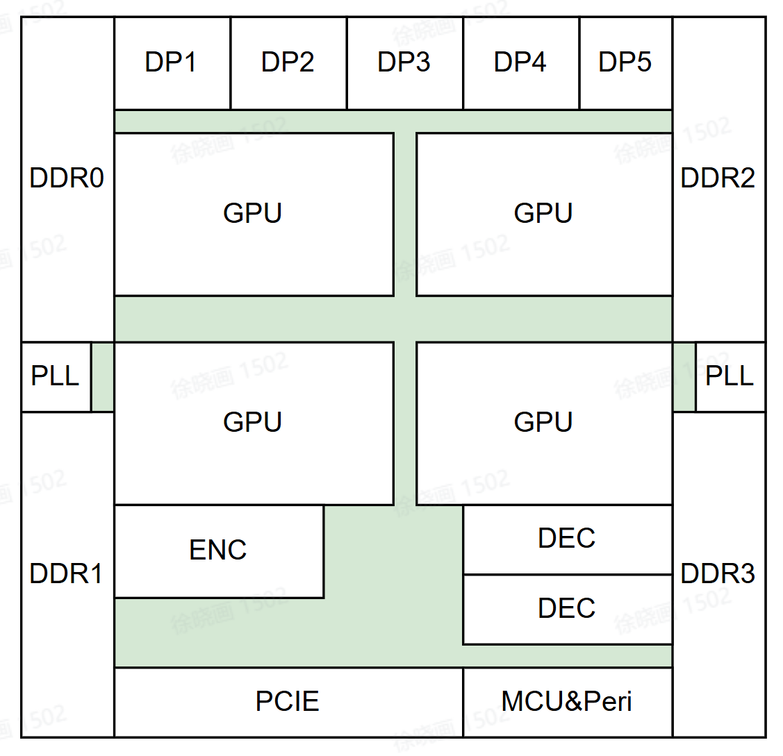
GPU cores with DDR4/LPDDR4 support, DP x6 4K@60Hz, VPU encoder/decoder, RISC-V MCU, comprehensive peripheral interfaces, 14x14mm.
Discuss your semiconductor design requirements with our engineering experts.